Bypassing Read-out Protection on the STM8S103
TLDR: I tried dumping the firmware of a read-out protected STM8S103 with voltage glitching. First I thought capacitors are for losers, then found out I need them, then picked a capacitor an order of magnitude too large, and finally replaced the capacitor with an external power supply to make the glitch work and dump the firmware.
Motivation
In my previous post about building an EMFI setup, I mentioned that my interest in fault attacks was sparked by a read-out protected (ROP) STM8 microcontroller, found on a printer’s display controller PCB. Almost a year passed before I finally found the time to tackle the project. After submitting my bachelor’s thesis this February, I finally had some free time available, and immediately dove into the project.
Previous Work
There already exist multiple sources about glitching the STM8:
- write-up by rumpeltux: first one I found with valuable information but little details
- examples section of findus project: about glitching a custom UART bootloader implementation; not ROP
- write-up by Jarrett: about glitching ROP with a 555 timer circuit; funny read but too much effort
- write-up by monte-monte: fairly detailed write-up with a lot of valuable information; (ends up disabling the internal voltage regulator and doing voltage multiplexing instead of simple crowbar glitching)
- chip.fail talk by Thomas Roth and Josh Datko: probably the best introduction to voltage glitching on a budget out there
However, after reading through all of these and trying to replicate it on my own STM8S103, it simply would not work, so I decided to write yet another post about it.
STM8S103
The STM8S103 is a low-cost, 8-bit MCU with up to 16KB of flash, integrated timers, ADC, UART/SPI/I2C peripherals, and most importantly for this article, a hardware-enforced ROP.
Programming and debugging the MCU is done via ST’s Single Wire Interface Module (SWIM), which, as the name implies, only needs one data line for its operations. It has only three commands: reading, writing and resetting the MCU.
The memory map looks like the following. (Note, that I left out some Reserved blocks for brevity; check the datasheet for the full map.)
| Start | Description |
|---|---|
| 0x0000 | RAM / Stack (1KB) |
| 0x4000 | EEPROM |
| 0x4800 | Option bytes (11 bytes) |
| 0x4865 | Unique ID |
| 0x5000 | GPIO / Peripheral registers |
| 0x7F00 | CPU/SWIM/debug/ITC registers |
| 0x8000 | Flash program memory (8KB) |
The first byte of the Option bytes block is the actual ROP byte. When set to 0xAA the read-out protection is enabled, causing every read access via the SWIM interface to return 0x71. (This value is not documented anywhere in the three documentations I found about the STM8 and SWIM btw.) Erasing the ROP byte, causes the EEPROM, Option bytes, and flash memory to be cleared immediately.
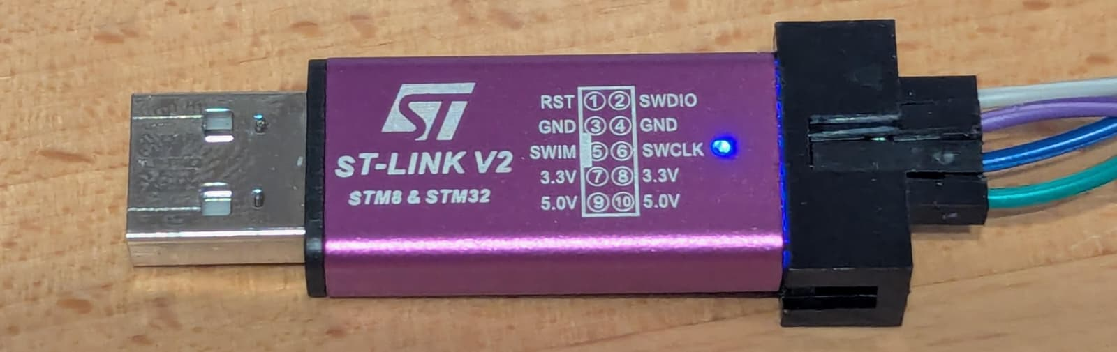
To read out the firmware from the flash memory, I used an STLinkv2 adapter. The adapter communicates with the MCU over the SWIM interface and requests some amount of bytes (max. 255 per request).
If we are allowed to read, i.e. ROP != 0xAA, the MCU sends back the requested bytes. Note, that the ROP byte is not checked for every read request, but rather a “protect memory flag” is latched once at startup. This can be easily verified by enabling ROP without resetting the MCU afterwards: reading the entire memory is possible until the chip is reset.
This implies that we only have to glitch successfully once during the startup phase to read the entire memory, which sounds doable judging by the following sentence from the datasheet.
Even if no protection can be considered as totally unbreakable, the feature [ROP] provides a very high level of protection for a general purpose microcontroller.
Voltage Glitching
Voltage glitching is a fault injection technique that disturbs the power supply of a target device in order to trigger unintended behavior like altering the regular control flow of a program or corrupting memory contents. There are three general approaches to voltage glitching: Arbitrary Waveform Glitching, Voltage Multiplex Glitching, and Crowbar Glitching1.
Arbitrary waveform glitching was first introduced in 2019 and, as the name implies, inserts arbitrary waveforms into the supply lines of a target. It’s probably the most powerful form of voltage glitching but requires a rather complicated setup.
Another technique with a rather sophisticated setup is voltage multiplex glitching, where the attacker quickly switches the voltage levels of the targets power lines. I couldn’t find much information about this technique besides some info in the examples section of the findus library.
Crowbar glitching is, setup-wise, the easiest technique and therefore what we will be doing in this article. It was first introduced in a paper by Colin O’Flynn in 2016, where he showed successful attacks against five devices using this method. It involves shorting the power rails of the target for a very short amount of time; typically in the nano- to microsecond range. Shorting the rails is usually implemented by connecting an N-channel MOSFET between VDD and GND, like shown below.
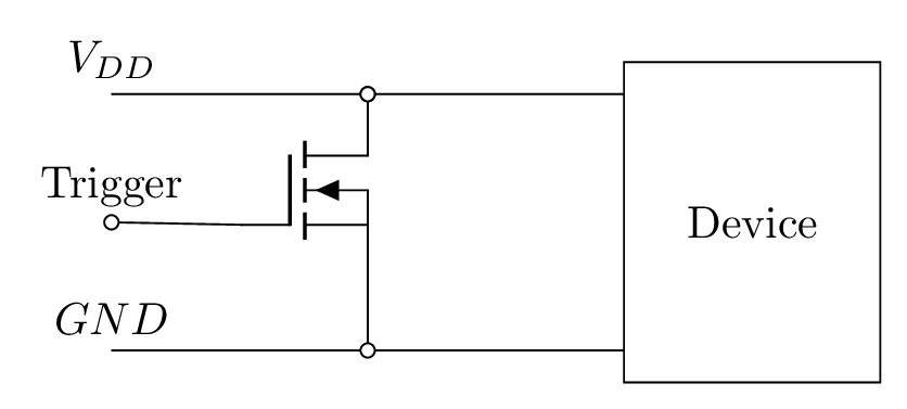
When trigger is HIGH, VDD is pulled to GND, resulting in a voltage drop in VDD. This can cause timing violations in the target device.
The desired effect of a crowbar glitch in our scenario is to disturb the latching of the “protect memory flag” mentioned in the previous section. How this can happen exactly cannot be determined without access to the inner workings of the internal state machine responsible for the ROP mechanism. However, several stages during the start-up phase could potentially be affected by a glitch. Possible points where the ROP mechanism may be vulnerable to a crowbar glitch include:
- Loading the ROP byte from memory
- Comparing its value to
0xAA - Latching the result
Target Preparation
Our target for the rest of this post will be a STM8S103F3 development board, which was maybe manufactured by ST Microelectronics. I say maybe, as I’m not 100% sure whether the MCUs on the development boards I bought from AliExpress are genuine. The functionality I cared about works just as described in the datasheet; however, the chip markings scream fake chip. Below picture shows the markings of a genuine STM8S003 on the left and the markings of the STM8S103 I received on the right.
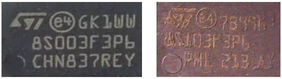
As you can see, the markings on the right chip are extremely blurry and barely readable. According to this source, out-of-spec ICs that were rejected during testing due to insufficient performance can enter the gray market. Such parts may be bought cheaply and then (sometimes poorly, sometimes not so poorly) remarked before being resold. Fingers crossed this doesn’t come back to bite me later.
Where to attack?
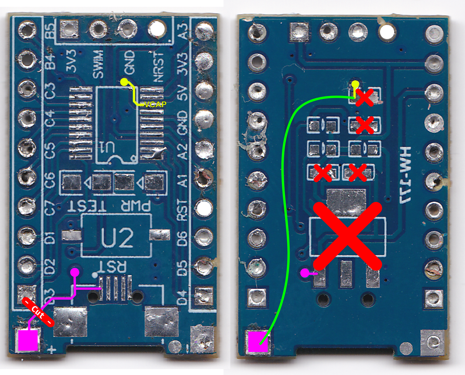
Below you can see an image of the development boards front side (left) and the back side (right). (Note, that I removed all components to have a better view on the traces; also the back side image is mirrored!). The most important traces and components are labeled.
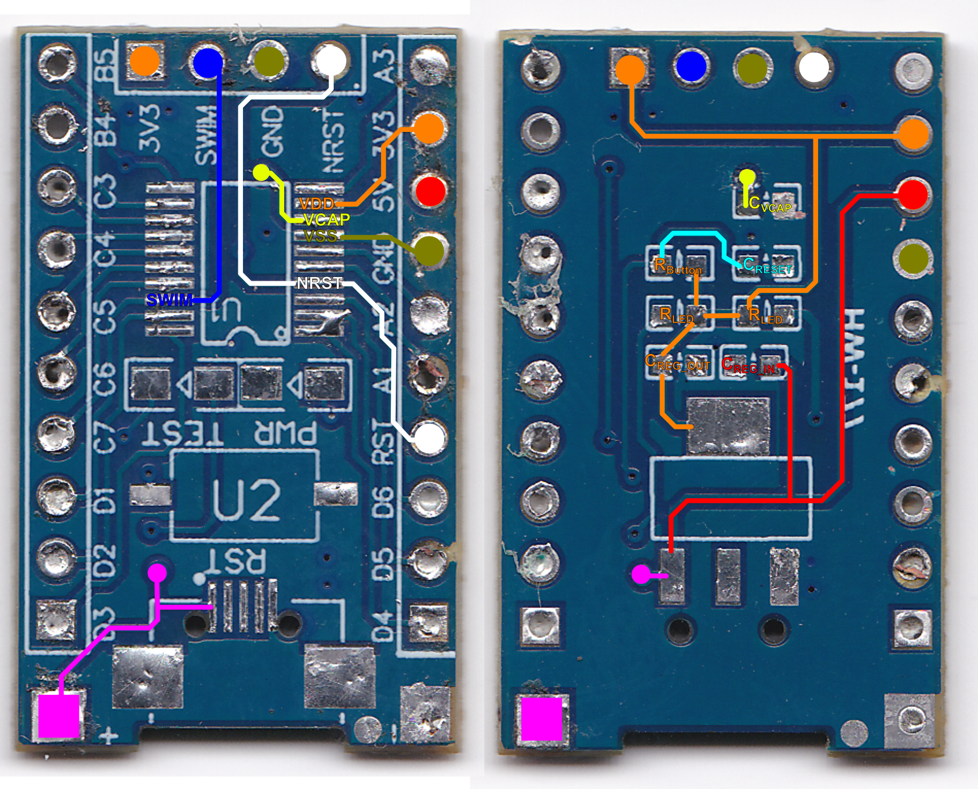
The yellow trace connects C_VCAP directly to the internal voltage regulator, which powers the CPU core. As the CPU core supply is sensitive to voltage fluctuations, transient disturbances at VCAP can affect instruction execution and potentially disrupt security mechanisms, resulting in unintended system behavior [source; image below derived from there too].
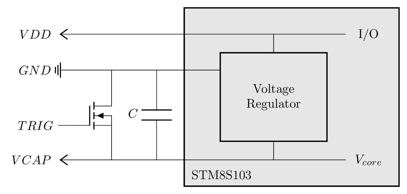
So VCAP will be our attack point: by shorting VCAP to GND, we can directly mess with the internal core voltage!
Changes to the PCB
All modifications I made to the target board are illustrated below. For good measure I removed all capacitors on the board and the external voltage regulator as they aren’t strictly required for operation (right?). Additionally, to have better access to the VCAP line, I cut the trace to the bottom left pad labeled with + and hacked in a wire.
Glitch Setup
With the target board suitably butchered, it was time to set up the actual glitching hardware. BTW: Most of the code I wrote for this project can be found in the project repository.
Hardware
Some time last year, I bought a Pico Glitcher v2.3, designed by Matthias Kesenheimer, for an insanely low price of 5 euro. The price was this low as it had some minor design error. Despite having a fully featured glitching platform readily available, I decided to devise my own setup from scratch, as I wanted to get started with FPGA programming anyway.
A simple crowbar glitching device should be capable of four things:
- Starting the glitch based on an input trigger
- Delaying the glitch from the input trigger signal for some amount of time
- Shorting the power rails of the target for some amount of time
- Update the glitch parameters during runtime
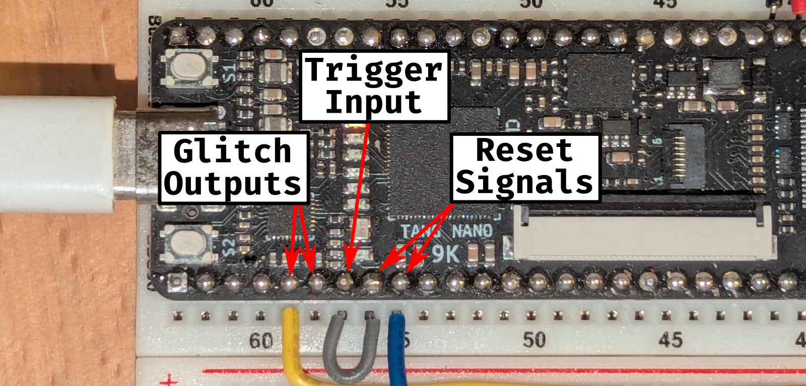
So I started implementing a simple glitcher on a Tang Nano 9K FPGA development board. One major problem I came across was that my design did not work for a 108MHz clock, as I did the initial development on the standard internal clock 27MHz. When trying to step up from 27 to 108Mhz the toolchain threw this error:
ERROR: Max frequency for clock 'sys_clk': 75.14 MHz (FAIL at 108.00 MHz)
which just means my code sucks so hard that it cannot be routed to fulfill the 108MHz timing constraints.
I tried synthesis with 81MHz (3 x 27MHz), and the glitcher worked despite the timing violation reported by the toolchain! Initially, I was worried that the resolution wouldn’t be enough to trigger successful glitch, but that turned out not to be a problem.
Software
After coding a python interface for the glitcher, I wanted to use it with the findus fault injection library (mainly for the nice graphical output it provides). So after writing yet another interface I was ready to write the actual glitching logic.
The glitching script does four things:
- set random glitch parameters
- start glitcher (listen for reset signal)
- reset chip (actually starts the glitch)
- check if ROP was glitched
To check whether ROP was glitched successfully I used stm8flash_dump, which adds an additional command line flag to do exactly this to the original stm8flash tool.
Glitching!!!
Finally it was time to start glitching…
No capacitor?
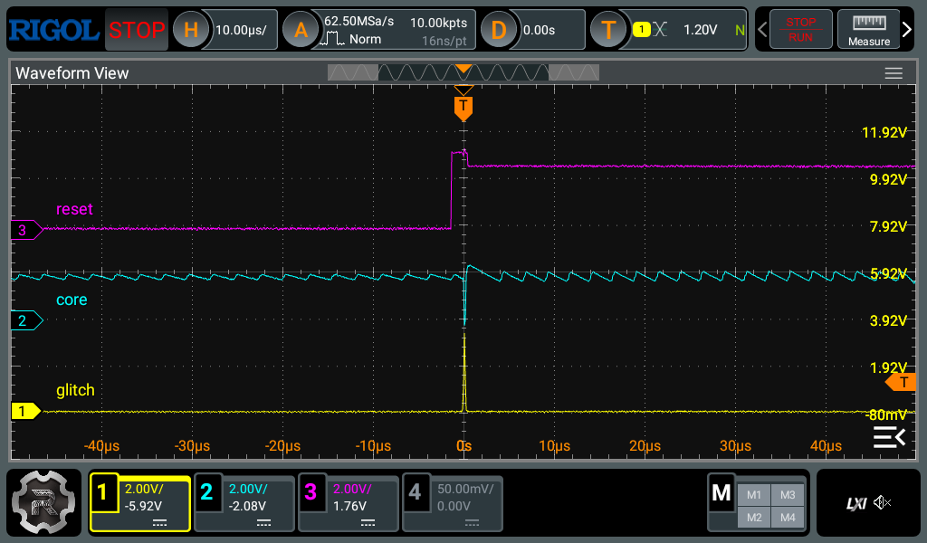
Below we see a first test glitch, with no capacitor installed. First the reset line (purple) is pulled low to hold the MCU in reset. When reset is released, a delay of 100 clock cycles (~1,24ms @ 81MHz) is applied before the glitch line (yellow) is pulled high for 13 clock cycles. During these 13 clock cycles we can observe the core voltage (cyan) dropping for roughly the same duration. Thats the effect we want to see.
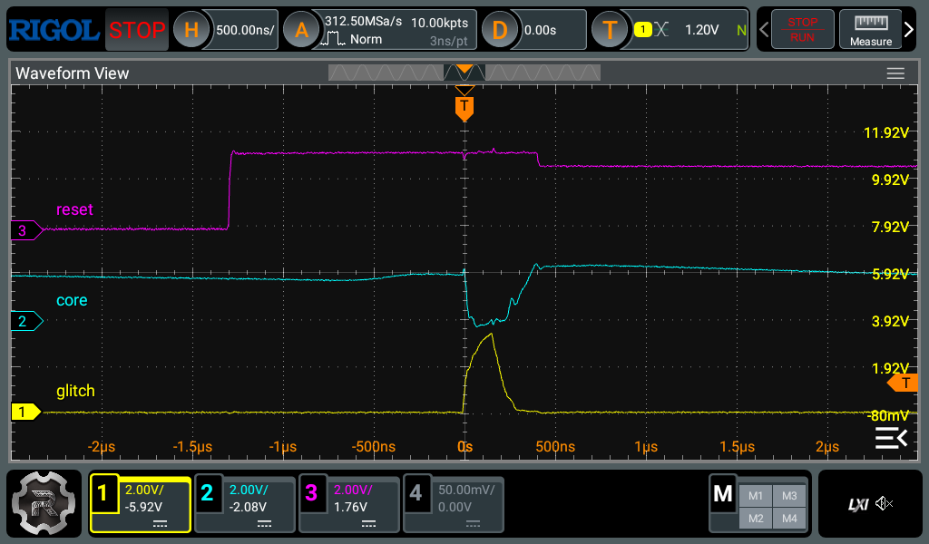
However, what we don’t want to see is the reset line also dropping slightly at around 400ns. That means that the core voltage is too low for the chip to continue operation, which prevents us from reading out the memory after a successful glitch.
When zooming out to to inspect more of the core voltage we can see a clear sawtooth pattern of the core voltage, indicating that the core voltage is highly unstable.
Zooming out even more reveals that the chip resets even without us glitching in between (e.g. at t=100us, t=150us, t=200us).
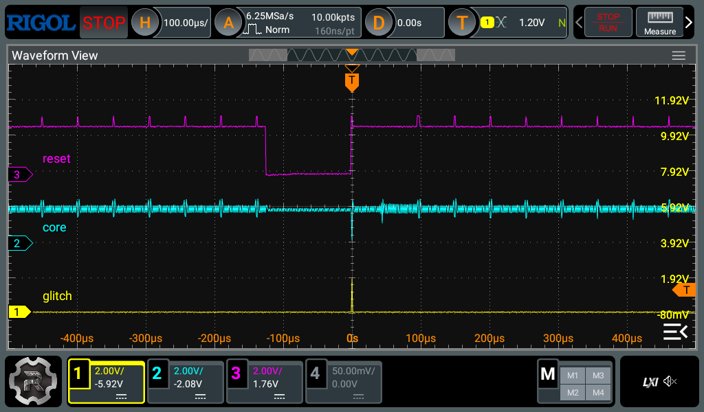
This behavior makes sense as the datasheet clearly states that we need a capacitor on the VCAP line between 470nF and 3300nF.
Because I didn’t have such small capacitors on hand, I inserted a 10uF (left image) and a 100uF capacitor (right image) on the VCAP line, with 30 clock cycles glitch duration. Note, that the core voltage on the left drops more than on the right (Vmin=216mV vs. Vmin=800mV), which makes sense to me as the 10uF capacitor stores less energy than the one with 100uF, resulting in a larger drop.
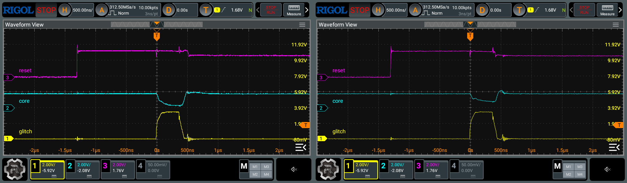
So we do in fact need a capacitor on VCAP to prevent the chip from resetting, but it should be as small as possible to achieve a sufficiently powerful glitch.
No SWIM Zone
Finally the time has come to find a successful glitch… or so I thought.
The datasheet states that the maximum time from reset pin release to vector fetch is 150us. As the ROP byte has to be checked before any code is executed on the system, I continued to use this as the upper bound for the delay parameter bruteforce. For the glitch length I chose an upper limit of 12 clock cycles, as the chip always resets with glitches above 12 clock cyles. The result from this bruteforce search, including about 10.000 attempts, are depicted below.
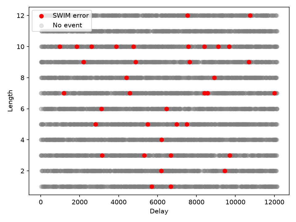
The STLink reported 36 SWIM errors, meaning there was some problem with the communication over the SWIM interface. What problem exactly is impossible to say with the current setup as stm8flash only reports a generic error message.
In hindsight this attempt was really stupid. The datasheet CLEARLY states the minimum (470nF) and maximum (3300nF) values for
VCAP… and I tried my luck with a 10uF capacitor🗿.
Voltage Regulators
After a very long time of trial and error I came across the Tips and Tricks section of the chipwhisperer wiki about “Targets with Internal Regulators”. The short article is originally about preventing internal regulators from distorting measurements in side-channel power analysis setups by using an external voltage source to overpower the chip’s internal voltage regulator. The idea is that the internal regulator sees that the feedback voltage is above the target voltage (1.8V in our case) and thus will not pass any voltage, resulting in a lower noise signal.
I suspected this might also be useful for voltage glitching: perhaps the internal regulator would take longer to compensate for the crowbar glitch when its feedback voltage was above 1.8V. (I don’t know if this is actually what happens internally, but it seemed to work.)
So I threw out the 10uF capacitor, set my power supply to 1.9V, and hooked it up directly to the VCAP line. And et voilà…
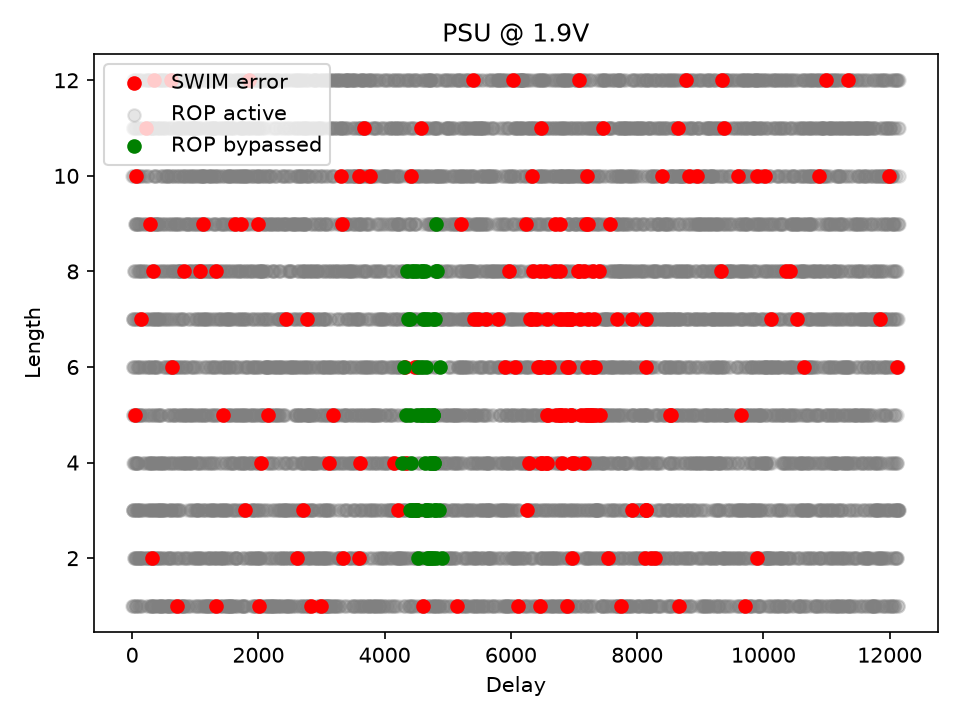
The green points mean that the read-out protection was bypassed and the memory read out successful!!!
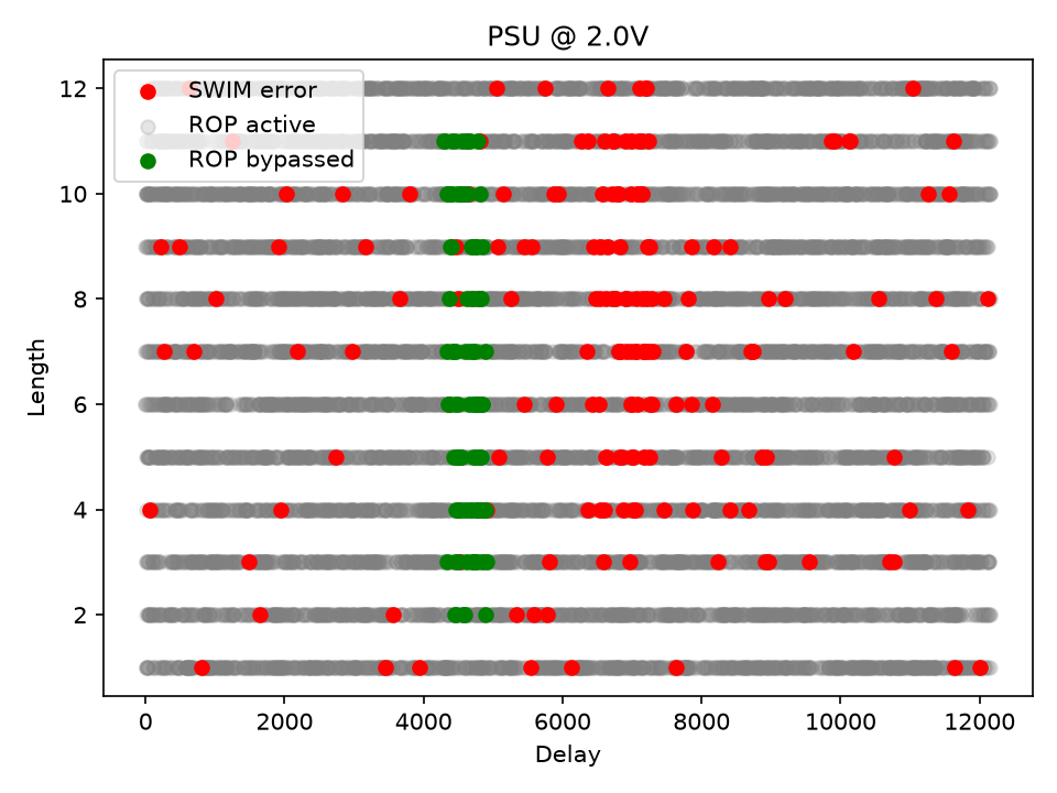
Overall, we achieve a success rate of around 11%, with delays between 4000 and 5000 clock cycles (approximately 50-60us at 81MHz) and glitch lengths ranging from 2 to 8 clock cycles. Increasing the voltage to 2.0V results in slightly more successful glitches and allows for longer glitch lengths as well (see Appendix A).
To avoid releasing the magic smoke, I refrained from increasing the voltage any further.
Profit??
Now, finally, after more than a year of waiting, it was time to dump the firmware from the printer display controller; the very thing that had sparked this whole ordeal. So I desoldered the chip from the display controller and stuck it on a breakout board.
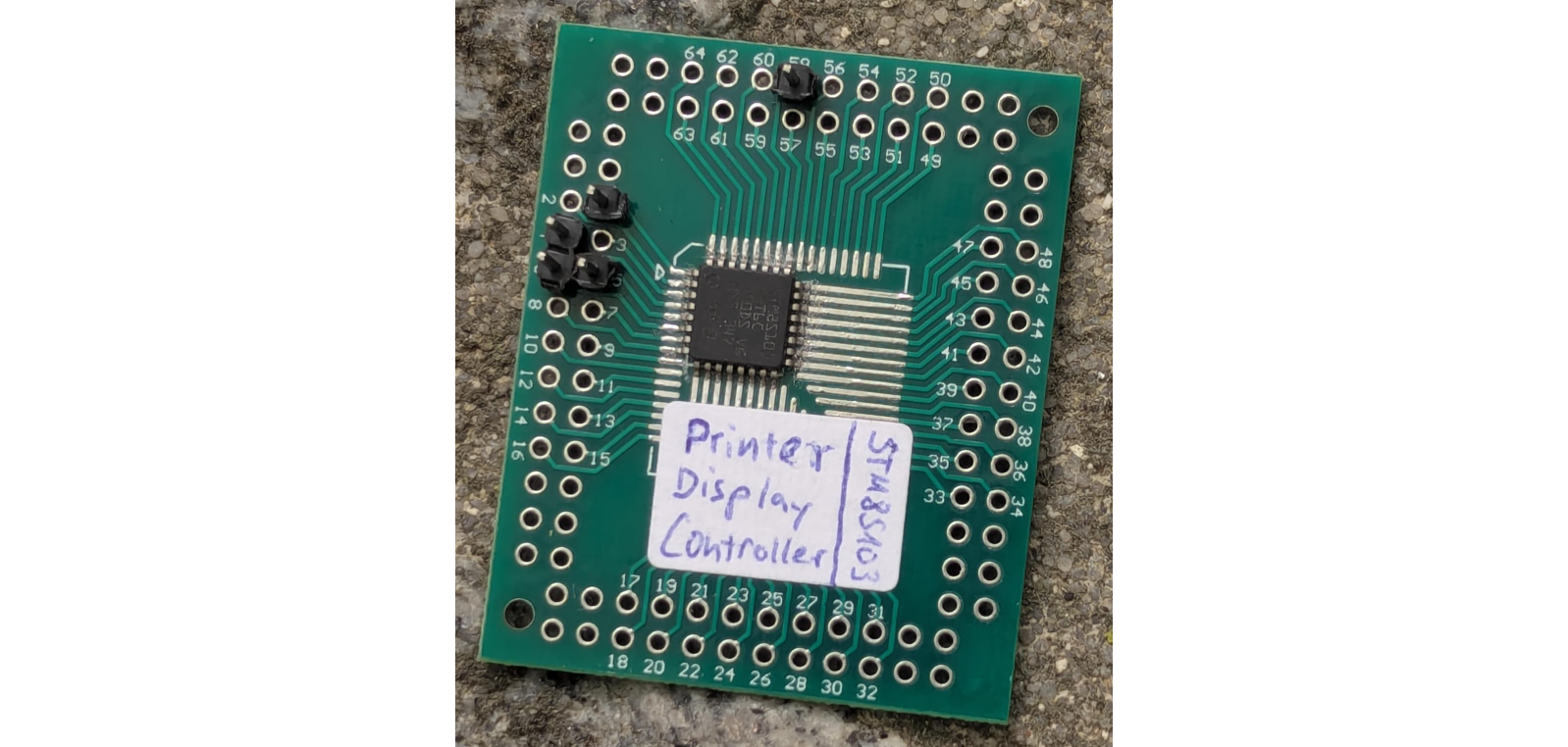
At this point, I was really worried that it wouldn’t work for some reason. My biggest concern was the obviously counterfeit chip I’d done my entire testing phase with.
But it worked.
Just as with the test device :)
Conclusion
After a lot of trial and error, I was finally able to bypass the read-out protection on the STM8S103 using a relatively simple setup. I learned a lot about crowbar voltage glitching and even learned some verilog on the way.
The biggest lesson from this project is just how sensitive voltage glitching is to the physical setup. Seemingly minor changes to the setup (not even only the circuit) can have a huge impact on the resulting glitch (see Appendix B).
This also explains why reproducing results from other STM8 glitching write-ups was much harder than expected. Even when the general attack methodology is the same, the exact parameters that work can be highly specific to the hardware and wiring of the individual setup. In my case, the external VCAP supply turned out to be the key to making the attack work, although it probably also would have worked with a smaller capacitor (or even using the original one, lol).
EDIT (2026-08-20): I tried again with a 100nF capacitor on VCAP with the external power supply disconnected. The chip worked without repeated resets, even though the datasheet gives a minimum capacitance of 470nF. However, I still didn’t observe any successful glitches. Some people in the comment section of rumpeltux’ writeup recommended to raise the supply voltage. Therefore I raised it to 6.5V (maximum rating is 5.5V!), but this didn’t produce any successful glitches either. Apparently, there is also the possibility of leaving VDD disconnected, only provide 1.8V at VCAP and then glitch with voltage multiplexing. The catch is that they used a different MCU (STM8S005) and I’m not sure if it applies to this MCU as well. I wasn’t able to read out the chip at all when providing only 1.8V at VCAP, either.
Appendix
A. Increasing PSU Voltage
Glitch frequency increases slightly with applied voltage, but point in time stays the same.
B. Many Different Glitches
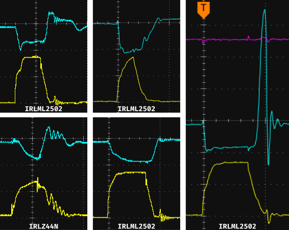
During the numerous hours of attempting to glitch the ROP I observed multiple different glitch traces. All of them were generated by seemingly identical setups. However, I noticed that the exact behavior of my setup is extremely unpredictable. Simply using a different cable on the breadboard can completely change the resulting trace. Sometimes, it even felt like the setup changed randomly overnight just to mess with me.
Below are five different traces I recorded: four generated using an IRLML2502 transistor and one using an IRLZ44N transistor.
C. Full Setup
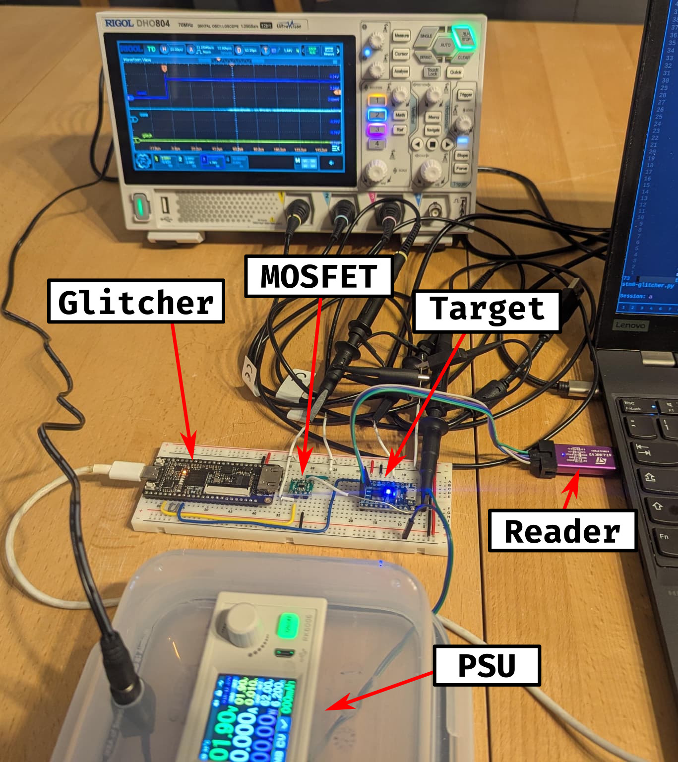
Footnotes
-
Most information in the Voltage Glitching section comes from the first two chapters of Shaping the Glitch: Optimizing Voltage Fault Injection Attacks and Fault Injection using Crowbars on Embedded Systems. For an in-depth explanation of how crowbar glitches work, I recommend Injecting Software Vulnerabilities with Voltage Glitching. ↩